JVD™ Solders
Gold-tin solder alloys, with compositions ranging from the eutectic 80/20 Au/Sn to 73/27, are used for integrated circuit chip or die bonding, because of their high bond strength, adhesion, resistance to creep, low stress, corrosion resistance, good thermal conductivity and absence of whisker formation. Solder preforms are costly, and become difficult to use as required sizes shrink. Solder pastes can have both process capability issues and shortcomings in high performance device reliability and durability.
JVD™ thin film AuSn solder layers offer a manufacturable solution.
We use the JVD process to deposit eutectic AuSn solder layers with thicknesses typically from 1 to 10 microns, and have deposited over 20 microns. Alloy composition is precisely maintained from source to substrate as we deposit the alloy; our process does not deposit alternating Au and Sn layers. Metal capture efficiency can exceed 90% with little waste of expensive metal. We do batch or single part processing depending on the substrate, and can handle round wafers, ceramic squares and rectangles, Si and III-V wafers in sizes ranging from 2" to 8", down to the smallest submounts and heatsinks in custom holders. Patterned photoresists remain cool during our process with the vast majority of jobs not exceeding 120 degrees C.
We have the ability to deposit up to 4 different materials in a single run using JVD sources. For example, we can deposit adhesion / diffusion barrier / AuSn / Au layers in a continuous sequence without breaking vacuum.
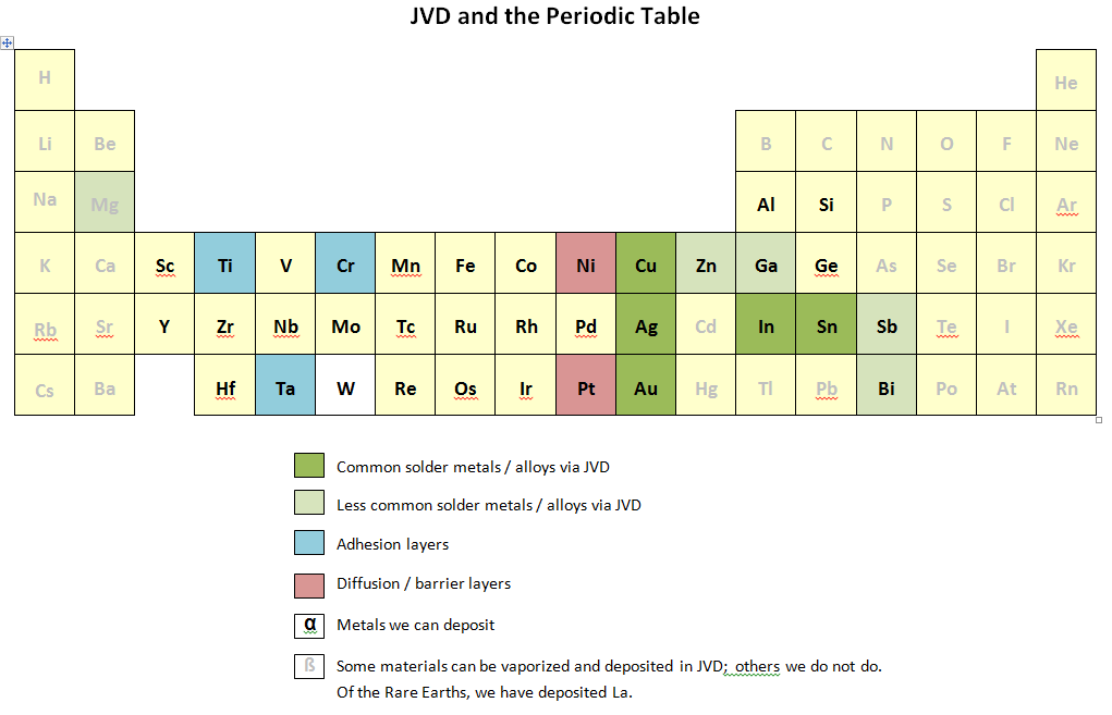
Lead free soldering has become a primary goal in advanced microelectronics, semiconductor packaging and related worldwide markets. We can deposit many of the elements of greatest importance in lead free solder such as Au, Ag, Sn, Cu, singly or in alloy form, with excellent control over alloy composition.
We can deposit solder bumps of extremely small size and high area density by high rate deposition of AuSn through patterned photoresist with feature sizes below 10 microns, e.g.: 4 X 4 microns with 8 micron pitch.
Related information on JVD advantages and capabilities for lead free solder deposition can be found in the Technology - JVD™ Processes section.
For additional information click here for the February 2003 article on JVD gold-tin solder in Advanced Packaging magazine.
For more information on offerings and pricing, please contact us.
For solder and ancillary metal deposition, the JVD approach, jet sources, and relative motion schemes provide many benefits.
|
WIDE RANGE OF SOLDERS |
These include AuSn 80/20 and some off-eutectics, 78/22, 75/25, 73/27; SnAg, SnCu, SnCuAg, SnIn, SnInAg -- most lead free solders used in microelectronics. |
|
ADHESION/BARRIER METALS |
Ti, Cr, Ta, Ni, TiPtAu, TiW, TiNiAu |
|
RELATED METALS |
Cu, Au, Ag, Sn, Al, Cr, Ni, Ti, Ta |
|
SUBSTRATE MATERIALS |
Virtually any substrate, since JVD is a "low vacuum" approach |
|
SUBSTRATE SIZE |
Wafers 2", 3", 4", 6", 8"; Square from 2"x2" to 6"x6" and rectangular substrates, down to small heatsinks of millimeter dimension |
|
SINGLE WAFER PROCESSES |
2" to 8" diameter or multiple substrates fitting into those areas |
|
BATCH PROCESSES |
4" wafers or 4"x4" batches of 10. Smaller substrates in batches up to 20 per run. Small heatsinks such as CuW, MoW, as many as hundreds per run in appropriate fixtures. |
|
THICKNESS RANGE |
All solders, 1 to 20 microns; adhesion/diffusion layers, typically 1,000 to 2,500 Å |
|
HIGH DEPOSITION RATES |
5 microns on a 6" wafer in 20 minutes for all solders. The "high" pressure of JVD implies high metal atoms concentration in jet; therefore, high deposition rates. |
|
ALLOY DEPOSITION |
Alloy components deposit together rather than as separate layers. |
|
ACCURATE COMPOSITION |
Metal vapor deposited from the jet preserves the starting alloy wire composition. |
|
THICKNESS CONTROL |
Plus/minus 10% across the wafer surface. |
|
"ION ETCH" PRE-CLEAN |
In situ low ion energy, high density plasma for residual resist removal. Other in situ pre-clean techniques include RF oxygen plasma and microwave discharge O atom exposure. |
|
MINIMAL MATERIAL WASTE |
Typical capture efficiencies in the jet are ~ 90%. |
|
LOW TEMPERATURE PROCESSING |
Fast relative motion of substrate keeps its temperature low because of short residence time in front of "hot" jet source. Maximum final wafer T of most single metal processes is less than 90°C. For multiple metal stacks, including those with high melt T materials, final wafer T can reach up to 110-120ºC. |
|
PHOTORESIST AND LIFTOFF COMPATIBILITY |
Low process T avoids thermal damage to photoresist mask. |
|
NANOCLUSTER DEPOSITION |
In the nozzle and jet, JVD flow and pressure conditions can be easily modified to promote nucleation, growth, and deposition of nanoclusters at very high rates. Cluster deposition, which is highly directional, is advantageous for solder bumps, because the high inertia of the accelerated, heavier clusters gives trajectories almost exactly perpendicular to the wafer. In consequence, there is little shadowing by resist walls, and since sidewall deposition is also reduced, there is reduced breadloafing. For small windows in the resist, where the aspect ratio is high, hole filling by nanoclusters is extremely efficient. In recent years, we have been putting this key nanocluster capability of JVD to increasing use in making small bumps in dense arrays. |
|
CLEAN AND GREEN OPERATION |
With starting materials of pure metals, there are no toxic precursors or effluents, and high capture efficiency minimizes waste. Nanocluster mode operation is particularly effective in concentrating the deposit. For additional information, click on the following link for the 2011 EPA SBIR success story in "Science Matters" newsletter: www.epa.gov/sites/production/files/2015-06/documents/jetprocess.pdf |
|
COMPACT DEPOSITION CHAMBERS |
The "Index Arm" JVD deposition tool in Figure 7 deploys JVD's solder deposition capabilities in a particularly concentrated form. Four different jet sources, for example, AuSn, Ti, Pt and Au are arranged in a circle, and the "index arm" permits a spinning wafer to visit and "scan" each source in turn to build up a complete layer. The ion etch pre-clean is integrated into the AuSn jet source. The entire chamber is ~ 16 liters (23" diameter, 6 inches high). |